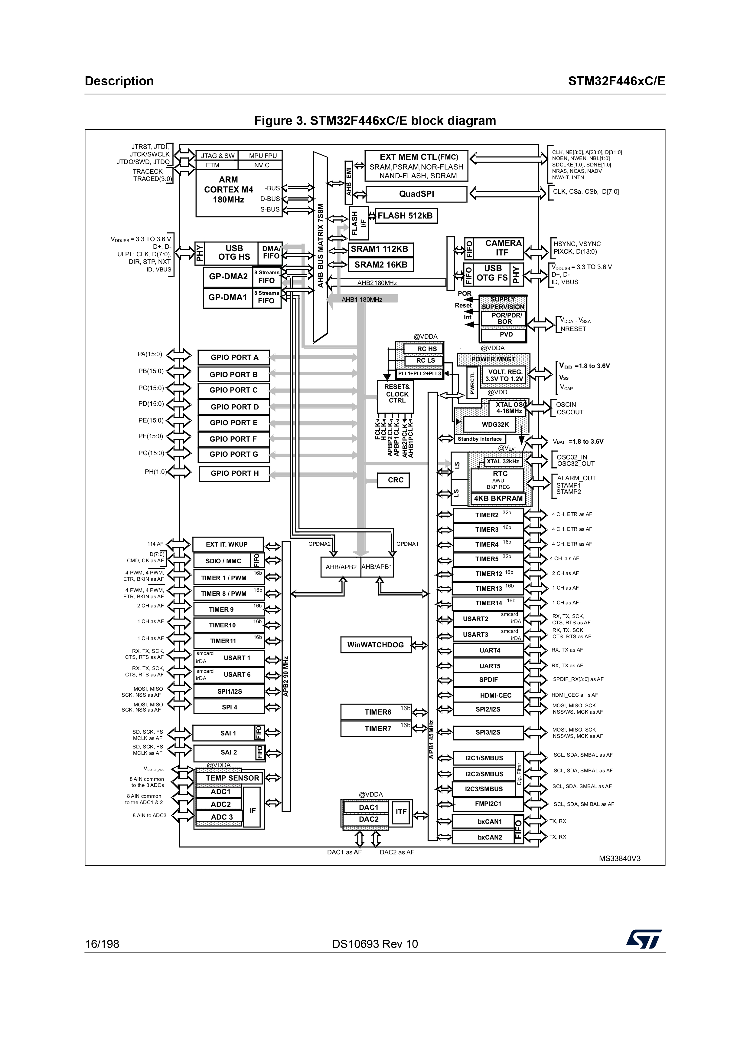
Buses are used to convey data. For the below tutorial, we’ll look at the STM32F446RE board.
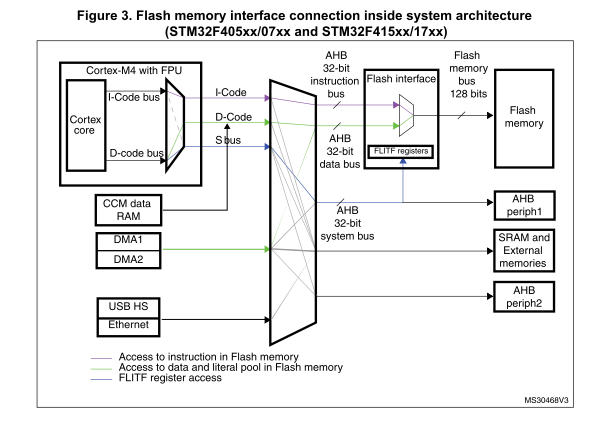
- I-bus: instruction bus, processor uses I-bus to fetch instructions from flash memory; manufacturer makes sure flash is connected to I-bus
- D-bus: data bus, processor uses d-bus to read data stored in flash, such as constant data
- S-bus: system bus Bus interfaces are restricted to accessing a certain range of addresses. For ARM Cortex M-4 processor, for example,
- If instructions are present between memory locations 0x000000 to 0x1FFFFFFC then processor fetches instructions using I-CODE interface
- If data is present between memory locations 0x000000 to 0x1FFFFFFF then processor fetches data over D-CODE interface
- S-bus can be used to access instructions or data when the other two buses cannot; peripherals for example must be talked to using system bus
- System bus is “extended” to run at higher speeds using the bus matrix; a “bridge” converter converts from AHB to APB1/APB2 protocol - 180 mHz downgraded to 45 mHz/90 mHz. GPIO hangs off of AHB bus, meaning it can run at 180 mHz. However the peripherals hang off of the APB bus, which means they are slow peripherals.
- Note that I-bus, D-bus can only read from flash, while S-bus reads from SRAM. Therefore, instructions/data can be read simultaneously from flash, whereas the same is not true for SRAM (two vs. one bus line).
Why are there two bus lines?
The reason has to do with needing two caches:
Data management
Literal pools are fetched from Flash memory through the D-Code bus during the execution stage of the CPU pipeline. The CPU pipeline is consequently stalled until the requested literal pool is provided. To limit the time lost due to literal pools, accesses through the AHB databus D-Code have priority over accesses through the AHB instruction bus I-Code. If some literal pools are frequently used, the data cache memory can be enabled by setting the data cache enable (DCEN) bit in the FLASH_ACR register. This feature works like the instruction cache memory, but the retained data size is limited to 8 rows of 128 bits.
Note that the processor is attached to all of those buses.
Constant data is stored in ROM - Read only memory, flash memory of the microcontroller. Consts are in the read-only section of the final executable. In contrast, non-constant data is stored in SRAM.
Aside: HCLK is the main CPU clock. It’s also used for AHB bus interface. P1CLK/P2CLK are the clocks of APB1 and APB2 respectively.
Q: What is the bus matrix? Bus matrix is a “traffic controller” that routes and connects different busses together. What does it mean to serialise the access?
The 32-bit multi-AHB bus matrix interconnects all the masters (CPU, DMAs, USB HS) and the slaves Flash memory, RAM, QuadSPI, FMC, AHB and APB peripherals and ensures a seamless and efficient operation even when several high-speed peripherals work simultaneously.
Q: Can USB OTG peripheral and GPIOs communicate with the processor concurrently? No; although there are two independent lines for USB OTG and GPIO, they must both go through the system bus - which serialises access requests, processing one at a time - to reach the processor.
Q: Can the processor talk to flash memory and SRAM simultaneously? Yes; the I-bus or D-bus can be used to talk to flash memory, while the S-bus can be used to talk to SRAM.
Question
What is the difference between RAM and SRAM? What is a bus protocol? AHB Lite?
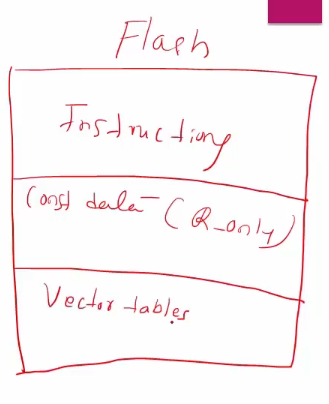 Interrupt vector tables
Attachments